Q.1.
Match the following:
| List I (Instrument) | List II (Measured quantity) | ||
|---|---|---|---|
| A. | Hot wire | 1. | only voltage |
| B. | PMMC | 2. | phase |
| C. | Electrostatic | 3. | true RMS value |
| D. | Lock in Amplifier | 4. | dc value |
-
A-3, B-2, C-1, D-4 -
A-1, B-4, C-2, D-3 -
A-3, B-4, C-1, D-2 -
A-2, B-3, C-4, D-1
Q.2.
Match the following:
| List I | List II | ||
|---|---|---|---|
| A. | Direct addressing | 1. | MOV A, M |
| B. | Register addressing | 2. | MOV C, A |
| C. | Register indirect addressing | 3. | LDA 7 |
| D. | Immediate addressing | 4. | STA FFC |
-
A-1, B-2, C-3, D-4 -
A-4, B-2, C-1, D-3 -
A-2, B-3, C-4, D-1 -
A-3, B-2, C-1, D-4
Q.3.
Match the following:
| List I | List II | ||
|---|---|---|---|
| A. | Zener diode | 1. |  |
| B. | Tunnel diode | 2. |  |
| C. | Schottky diode | 3. |  |
| D. | Diode | 4. |  |
-
A-1, B-3, C-2, D-4 -
A-2, B-3, C-1, D-4 -
A-4, B-3, C-2, D-1 -
A-3, B-2, C-4, D-1
Q.4.
Match the following:
| List I | List II | ||
|---|---|---|---|
| A. | Resistance | 1. | M-1L-2T4I2 |
| B. | Inductance | 2. | ML2T-2I-2 |
| C. | Capacitance | 3. | ML2T-3I2 |
-
A-1, B-2, C-3 -
A-2, B-1, C-3 -
A-2, B-3, C-1 -
A-3, B-2, C-1
Q.5.
Match the following:
| List I | List II | ||
|---|---|---|---|
| A. | Direct addressing | 1. | MOV A, M |
| B. | Register addressing | 2. | MOV C, A |
| C. | Register indirect addressing | 3. | LDA 7 |
| D. | Immediate addressing | 4. | STA FFC |
-
A-1, B-2, C-3, D-4 -
A-4, B-2, C-1, D-3 -
A-2, B-3, C-4, D-1 -
A-3, B-2, C-1, D-4
Q.6.
Match the following:
| List I | List II | ||
|---|---|---|---|
| A. | TV | 1. | 1 kHz |
| B. | Radio | 2. | 3 kHz |
| C. | Telephony | 3. | 9 kHz |
| D. | Telegraphy | 4. | 5 MHz |
-
A-4, B-1, C-2 -
A-4, B-3, C-2 -
A-2, B-1, C-3 -
A-1, B-2, C-3
Q.7.
Match the following:
| List I (Bit Pattern) | List II (Register pairs) | ||
|---|---|---|---|
| A. | 00 | 1. | SP |
| B. | 01 | 2. | B-C |
| C. | 10 | 3. | D-E |
| D. | 11 | 4. | H-L |
-
A-1, B-2, C-3, D-4 -
A-2, B-3, C-4, D-1 -
A-2, B-3, C-1, D-4 -
A-4, B-3, C-2, D-1
Q.8.
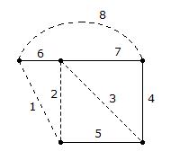
| List I (Branches) | List II | ||
|---|---|---|---|
| A. | 4 | 1. | Twigs |
| B. | 7 | 2. | Links |
| C. | 8 | 3. | Fundamental cutset |
| D. | 7 | 4. | Fundamental loop |
-
A-3, B-1, C-2, D-4 -
A-2, B-3, C-1, D-4 -
A-3, B-2, C-4, D-1 -
A-1, B-4, C-3, D-2
Q.9.
Match the following:
| List I | List II | ||
|---|---|---|---|
| A. | Direct addressing | 1. | MOV A, M |
| B. | Register addressing | 2. | MOV C, A |
| C. | Register indirect addressing | 3. | LDA 7 |
| D. | Immediate addressing | 4. | STA FFC |
-
A-1, B-2, C-3, D-4 -
A-4, B-2, C-1, D-3 -
A-2, B-3, C-4, D-1 -
A-3, B-2, C-1, D-4
Q.10.
Match the following:
| List I (Characteristics) | List II (Device) | ||
|---|---|---|---|
| A. | Voltage controlled device | 1. | BJT |
| B. | Current controlled device | 2. | UJT |
| C. | Conductivity modulation device | 3. | FET |
| D. | Negative conductance device | 4. | Impatt diode |
-
A-2, B-3, C-1, D-1 -
A-2, B-3, C-4, D-1 -
A-3, B-1, C-2, D-4 -
A-3, B-1, C-4, D-2
Q.11.
Match the following:
| List I | List II | ||
|---|---|---|---|
| A. |  | 1. | Slot line |
| B. |  | 2. | Coplanar line |
| C. |  | 3. | Microstrip |
-
A-1, B-2, C-3 -
A-3, B-2, C-1 -
A-2, B-3, C-1 -
A-3, B-1, C-2
Q.12.
Match the following:
| List I | List II | ||
|---|---|---|---|
| A. | Bode | 1. | Asymptotic plots |
| B. | Evans | 2. | Polar plots |
| C. | Nyquist | 3. | Root locus technique |
| 4. | M and N circles |
-
A-1, B-4, C-2 -
A-2, B-3, C-4 -
A-3, B-1, C-4 -
A-1, B-3, C-2
Q.13.
Match the following:
| List I (Characteristics) | List II (Device) | ||
|---|---|---|---|
| A. | Voltage controlled device | 1. | BJT |
| B. | Current controlled device | 2. | UJT |
| C. | Conductivity modulation device | 3. | FET |
| D. | Negative conductance device | 4. | Impatt diode |
-
A-2, B-3, C-1, D-1 -
A-2, B-3, C-4, D-1 -
A-3, B-1, C-2, D-4 -
A-3, B-1, C-4, D-2
Q.14.
Match the following:
| List I (Network parameter) | List II (Measured under open-circuit conditions) | ||
|---|---|---|---|
| A. | Z11 | 1. |  |
| B. | A | 2. |  |
| C. | C | 3. |  |
| D. | Z22 | 4. |  |
-
A-1, B-4, C-2, D-3 -
A-3, B-4, C-2, D-1 -
A-1, B-2, C-4, D-3 -
A-3, B-2, C-4, D-1
Q.15.
Match the following:
| List I | List II | ||
|---|---|---|---|
| A. | Zener diode | 1. | |
| B. | Tunnel diode | 2. | |
| C. | Schottky diode | 3. | |
| D. | Diode | 4. | |
-
A-1, B-3, C-2, D-4 -
A-2, B-3, C-1, D-4 -
A-4, B-3, C-2, D-1 -
A-3, B-2, C-4, D-1
Q.16.
Match the following:
| List I | List II | ||
|---|---|---|---|
| A. | NPN transistor | 1. |  |
| B. | PNP transistor | 2. |  |
| C. | n channel JFET | 3. |  |
| D. | p channel JFET | 4. |  |
-
A-1, B-2, C-3, D-4 -
A-3, B-4, C-2, D-1 -
A-4, B-2, C-1, D-3 -
A-1, B-2, C-4, D-3
Q.17.
Match the following:
| List I | List II | ||
|---|---|---|---|
| A. | | 1. | Slot line |
| B. | | 2. | Coplanar line |
| C. | | 3. | Microstrip |
-
A-1, B-2, C-3 -
A-3, B-2, C-1 -
A-2, B-3, C-1 -
A-3, B-1, C-2
Q.18.
| List I (Branches) | List II | ||
|---|---|---|---|
| A. | 4 | 1. | Twigs |
| B. | 7 | 2. | Links |
| C. | 8 | 3. | Fundamental cutset |
| D. | 7 | 4. | Fundamental loop |
-
A-3, B-1, C-2, D-4 -
A-2, B-3, C-1, D-4 -
A-3, B-2, C-4, D-1 -
A-1, B-4, C-3, D-2
Q.19.
| List I (Branches) | List II | ||
|---|---|---|---|
| A. | 4 | 1. | Twigs |
| B. | 7 | 2. | Links |
| C. | 8 | 3. | Fundamental cutset |
| D. | 7 | 4. | Fundamental loop |
-
A-3, B-1, C-2, D-4 -
A-2, B-3, C-1, D-4 -
A-3, B-2, C-4, D-1 -
A-1, B-4, C-3, D-2
Q.20.
Match the following:
| List I (Logic) | List II (Characteristic) | ||
|---|---|---|---|
| A. | RTL | 1. | High fan out |
| B. | CMOS | 2. | Highest speed of operation |
| C. | I2L | 3. | High noise immunity |
| D. | ECL | 4. | Lowest product of power and delay |
-
A-4, B-3, C-2, D-1 -
A-4, B-3, C-2, D-3 -
A-3, B-1, C-4, D-2 -
A-3, B-4, C-1, D-2
Q.21.
Match the following:
| List I (Devices) | List II (characteristic) | ||
|---|---|---|---|
| A. | BJT | 1. | Voltage controlled negative resistance |
| B. | MOSFET | 2. | High current gain |
| C. | Tunnel diode | 3. | Voltage regulation |
| D. | Zener diode | 4. | High input impedance |
-
A-1, B-4, C-2, D-3 -
A-2, B-4, C-1, D-3 -
A-2, B-3, C-1, D-4 -
A-1, B-3, C-2, D-4
Q.22.
Match the following:
| List I | List II | ||
|---|---|---|---|
| A. | Fourier transform of a Gaussian function | 1. | Gaussian function |
| B. | Convolution of a rectangular pulse with itself | 2. | Rectangular pulse |
| C. | Current through inductor for step input voltage | 3. | Triangular pulse |
| 4. | Ramp function | ||
| 5. | Zero |
-
A-1, B-2, C-3 -
A-2, B-4, C-5 -
A-1, B-3, C-4 -
A-2, B-3, C-5
Q.23.
Match the following:
| List I (Amplifier coupling) | List II (Feature) | ||
|---|---|---|---|
| A. | RC | 1. | High voltage gain and impedance matching |
| B. | Inductive | 2. | Ability to amplify dc and low frequency signals |
| C. | Transformer | 3. | Minimum non-linear distortion |
| D. | Direct | 4. | Low collector supply voltage can be used |
-
A-4, B-1, C-3, D-2 -
A-3, B-4, C-1, D-2 -
A-1, B-2, C-3, D-4 -
A-4, B-3, C-2, D-1
Q.24.
Match the following:
| List I | List II | ||
|---|---|---|---|
| A. | T (Reflection coefficient) = 0 | 1. | (ZL - Zo)/(ZL + Zo) |
| B. | T = - 1 | 2. | ZL = Zo |
| C. | T = + 1 | 3. | ZL = 0 |
| D. | - 1 < T < + 1 | 4. | ZL = ∞ |
-
A-2, B-3, C-4, D-1 -
A-2, B-4, C-1, D-3 -
A-1, B-2, C-3, D-4 -
A-3, B-2, C-4, D-1
Q.25.
Match the following:
| List I (I/P - O/P relation) | List II (Property of the system) | ||
|---|---|---|---|
| A. | y(n) = x(n) | 1. | Nonlinear, non-causal |
| B. | y(n) = x(n2) | 2. | Linear, non casual |
| C. | y(n) = x2(-n) | 3. | Linear causal |
| D. | y(n) = x2(n) | 4. | Nonlinear causal |
-
A-1, B-4, C-3, D-2 -
A-3, B-2, C-1, D-4 -
A-1, B-2, C-3, D-4 -
A-3, B-4, C-1, D-2
Q.26.
Match the following:
| List I | List II | ||
|---|---|---|---|
| A. | TTL | 1. | Low propagation delay |
| B. | ECL | 2. | Low power consumption |
| C. | MOS | 3. | High packing density |
| D. | CMOS | 4. | Saturated bipolar logic |
-
A-4, B-1, C-3, D-2 -
A-4, B-3, C-1, D-2 -
A-4, B-3, C-2, D-1 -
A-3, B-1, C-4, D-2
Q.27.
Match the following:
| List I | List II | ||
|---|---|---|---|
| A. | Sky wave | 1. | parasitic elements |
| B. | Antenna feed | 2. | delta match |
| C. | Reflector | 3. | long-wire antenna |
| D. | Rhombic antenna | 4. | ionosphere |
-
A-1, B-3, C-4, D-2 -
A-2, B-1, C-3, D-4 -
A-1, B-2, C-3, D-4 -
A-4, B-2, C-1, D-3
Q.28.
Match the following:
| List I (Operator) | List II (Description) | ||
|---|---|---|---|
| A. | & & | 1. | Bitwise inclusive OR |
| B. | & | 2. | Bitwise AND |
| C. | | | | 3. | Logical AND |
| D. | | | 4. | Logical OR |
-
A-1, B-2, C-3, D-4 -
A-3, B-2, C-4, D-1 -
A-2, B-3, C-1, D-4 -
A-1, B-4, C-2, D-3
Q.29.
Match the following:
| List I (Memories) | List II (Characteristic) | ||
|---|---|---|---|
| A. | Static PLA | 1. | erasable, programmable |
| B. | CCD | 2. | ultra high speed |
| C. | ECL | 3. | stores large volume of data |
| D. | GAL | 4. | Does not need refreshing |
| 5. | Non-volatile |
-
A-4, B-3, C-2, D-1 -
A-4, B-2, C-3, D-1 -
A-5, B-1, C-2, D-3 -
A-3, B-5, C-2, D-1
Q.30.
Match the following:
| List I (F.T and F.S) | List II (Properties) | ||
|---|---|---|---|
| A. | Fourier Series | 1. | Discrete, Periodic |
| B. | Fourier Transform | 2. | Continuous, Periodic |
| C. | Discrete Time Fourier | 3. | Discrete aperiodic |
| D. | Discrete Fourier Transform | 4. | Continuous, aperiodic |
-
A-3, B-4, C-2, D-1 -
A-1, B-2, C-4, D-3 -
A-3, B-2, C-4, D-1 -
A-1, B-4, C-2, D-3